AI chips are pushing everything else off TSMC's most advanced production lines
Key Points
- In 2026, Nvidia, Google, Amazon, and AMD are all moving their AI accelerators to TSMC's N3 process at the same time. According to SemiAnalysis, TSMC has underestimated demand for years and won't be able to build enough capacity for at least two more years.
- AI wafers are expected to account for around 86 percent of N3 capacity by 2027. Weakening smartphone demand is freeing up capacity that gets redirected straight to AI chips.
- Memory is also scarce. HBM consumes roughly three times more wafer capacity per bit than standard DRAM, and with HBM4 that ratio gets even worse.
By 2027, 86 percent of TSMC's N3 capacity could go to AI accelerators, according to SemiAnalysis. Smartphones are becoming a buffer for overflow demand.
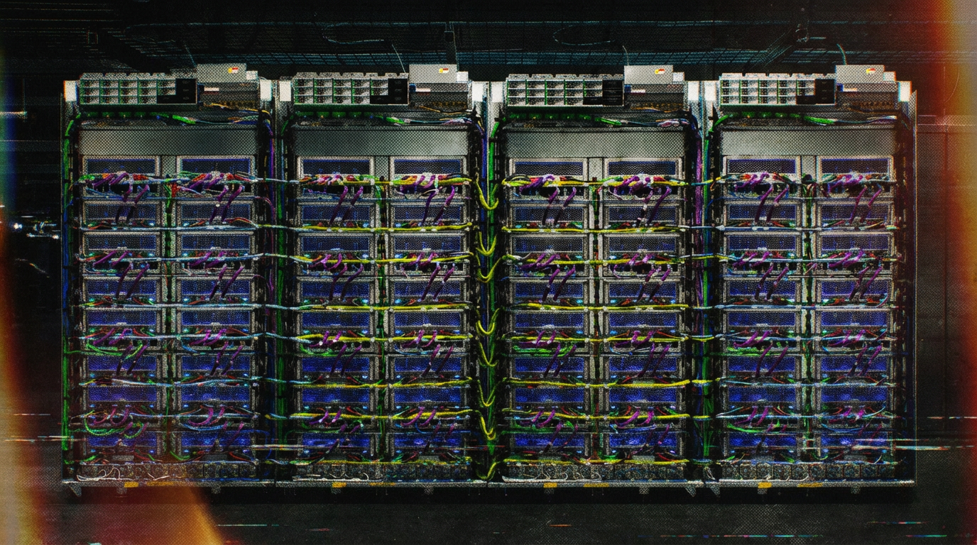
In 2026, nearly every major AI accelerator family is moving to TSMC's N3 manufacturing process at the same time - Nvidia's Rubin, Google's TPU v7/v8, Amazon's Trainium3, and AMD's MI350X. The resulting demand shock is hitting a foundry that simply can't expand fast enough. According to SemiAnalysis, TSMC has been caught flat-footed, with wafer capacity expansion falling well behind surging AI demand.
SemiAnalysis highlights just how badly TSMC misjudged AI demand. Even though the biggest compute buildout in history kicked off in late 2022, TSMC's capital expenditure didn't exceed its previous peak until 2025. Only now has TSMC recognized how far customer demand has outpaced its capacity, and the company plans to significantly surpass last year's record capex in 2026.
But even billions in additional spending won't fix the problem quickly, as new cleanrooms need to be built and equipped before extra capacity comes online. SemiAnalysis expects TSMC won't be able to add enough capacity to fully meet demand for at least the next two years.
N3 utilization is set to exceed 100 percent
The situation is so tight that effective N3 utilization is expected to surpass 100 percent in the second half of 2026, the analysts write. TSMC is already shifting certain process layers to other fabs to squeeze out incremental N3 capacity wherever possible. While AI-related wafers currently account for just under 60 percent of N3 output in 2026, that share is projected to hit 86 percent in 2027.
The smartphone industry is becoming what SemiAnalysis calls the release valve. Weakening consumer demand, driven by rising memory prices, is freeing up wafer capacity that gets redirected to AI accelerators. SemiAnalysis calculates that reallocating 25 percent of smartphone N3 wafer starts would enable production of roughly 700,000 additional Rubin GPUs or 1.5 million additional TPU v7s.
But more logic capacity alone won't solve the problem, as memory is also scarce. HBM consumes roughly three times more wafer capacity than standard DRAM, a gap that could widen to nearly four times as the industry transitions to HBM4.
AI News Without the Hype – Curated by Humans
As a THE DECODER subscriber, you get ad-free reading, our weekly AI newsletter, the exclusive "AI Radar" Frontier Report 6× per year, access to comments, and our complete archive.
Subscribe now