Chipmakers prepare for the angstrom age with successful tests of next-gen lithography machines
Belgian research company imec and ASML have successfully tested the next generation of machines for chip production.
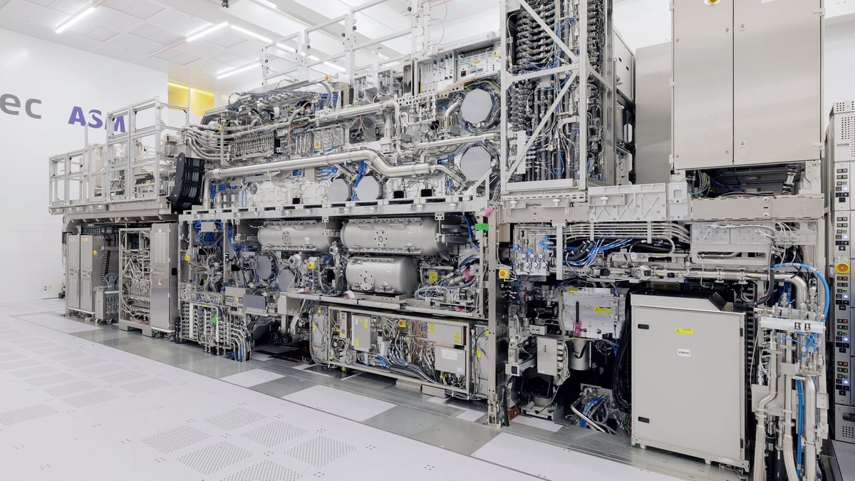
Researchers at the joint High-NA EUV lithography lab in Veldhoven, Netherlands, have succeeded in printing circuits as small or smaller than those currently used in commercial production of logic and memory chips in a single pass using the High-NA tool.
High-NA EUV lithography uses light beams with a higher numerical aperture (NA) to create smaller and more complex circuit structures on semiconductor wafers. This enables the production of faster, more powerful and more energy-efficient chips.
Technology for the "angstrom era"
Luc Van den hove, president and CEO of imec, emphasized the importance of this technology, stating that High NA will be "highly instrumental to continue the dimensional scaling of logic and memory technologies". The results confirmed the long-predicted resolution capability of High NA EUV lithography and paved the way for further advances in semiconductor technology that will push chip manufacturing into the "angstrom era".
In the semiconductor industry, this refers to the phase expected over the next few years in which chip production will be measured in angstroms rather than nanometers. Intel is already referring to its planned 2-nanometer chips as 20A (1 nm = 10 A), and the new technology should make its 14A chips possible.
The results show that chip manufacturers will be able to use ASML's High-NA system for their next chip generations in the coming years. Intel has purchased the first two High-NA systems, with a third to be delivered to TSMC this year. Other chip manufacturers such as Samsung Electronics, SK Hynix and Micron have also placed orders. Through TSMC, the technology will also be used by Nvidia for future AI hardware. Like the chips themselves, the machines are affected by US export bans, including to China.
AI News Without the Hype – Curated by Humans
As a THE DECODER subscriber, you get ad-free reading, our weekly AI newsletter, the exclusive "AI Radar" Frontier Report 6× per year, access to comments, and our complete archive.
Subscribe nowAI news without the hype
Curated by humans.
- More than 16% discount.
- Read without distractions – no Google ads.
- Access to comments and community discussions.
- Weekly AI newsletter.
- 6 times a year: “AI Radar” – deep dives on key AI topics.
- Up to 25 % off on KI Pro online events.
- Access to our full ten-year archive.
- Get the latest AI news from The Decoder.